News
Samsung’s 2nm tech promises smaller, faster, more efficient chipsets

Samsung says its 2nm chipsets will be smaller, faster, and more power efficient. The company is expected to begin mass production of semiconductors on a 2nm process. The advanced technology will offer multi-directional benefits.
2nm Samsung chipsets will be 17% smaller than the current generation. The products will also offer 18% performance improvement and 15% more efficiency. For the first time, a Samsung official explained the technological prowess of the BSPDN.
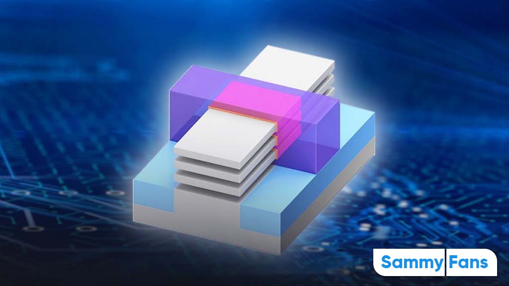
Advanced semiconductor production tech entered the foundry market as a backside power delivery network (BSPDN). It will reduce the size of a 2nm semiconductor by 17%, compared with the traditional front-end power delivery technology.
Samsung BSPDN reportedly places power rails on the back of the wafer to eliminate bottlenecks between the power and signal lines. As a result, the process manages to reduce the chipset’s size by a sharp 17 percent.

The Korean tech giant confirmed that it’s committed to its roadmap shared in 2022. Accordingly, the first 3nm mobile chip will be coming in the second half of the year, and deliver GAA on its upcoming 2nm process by the next year.
Samsung’s Exynos 2500 could be manufactured on SF3 (3nm) process tech. It is said to offer improved performance and power efficiency by 30% and 50%, respectively. The wafer size would also be reduced by 35% compared to 1st-gen GAA.
Intel plans to produce chips with BSPDN on the Intel 20A (2nm) process within the year. TSMC, which controls 62% foundry market, said it plans to introduce the BSPDN to its 1.6nm and below process nodes around the end of 2026.